With a highly experienced team and sophisticated equipment, we provide a precise solution to the analytical problems of solid materials, particularly in the semiconductor field.
Analytical Lab at the service of semiconductor industry for R&D and production
Our analysis service is widely and successfully used for the characterization of silicon and compound semiconductors as well as their related materials : metal and dielectric films.
The valuable and timely characterization data provided by us such as dopant impurity concentrations, thickness, structure, composition and interface quality in semiconductor devices are directly used to enhance the chip production yield and to reduce the R&D cycle time for our customers.
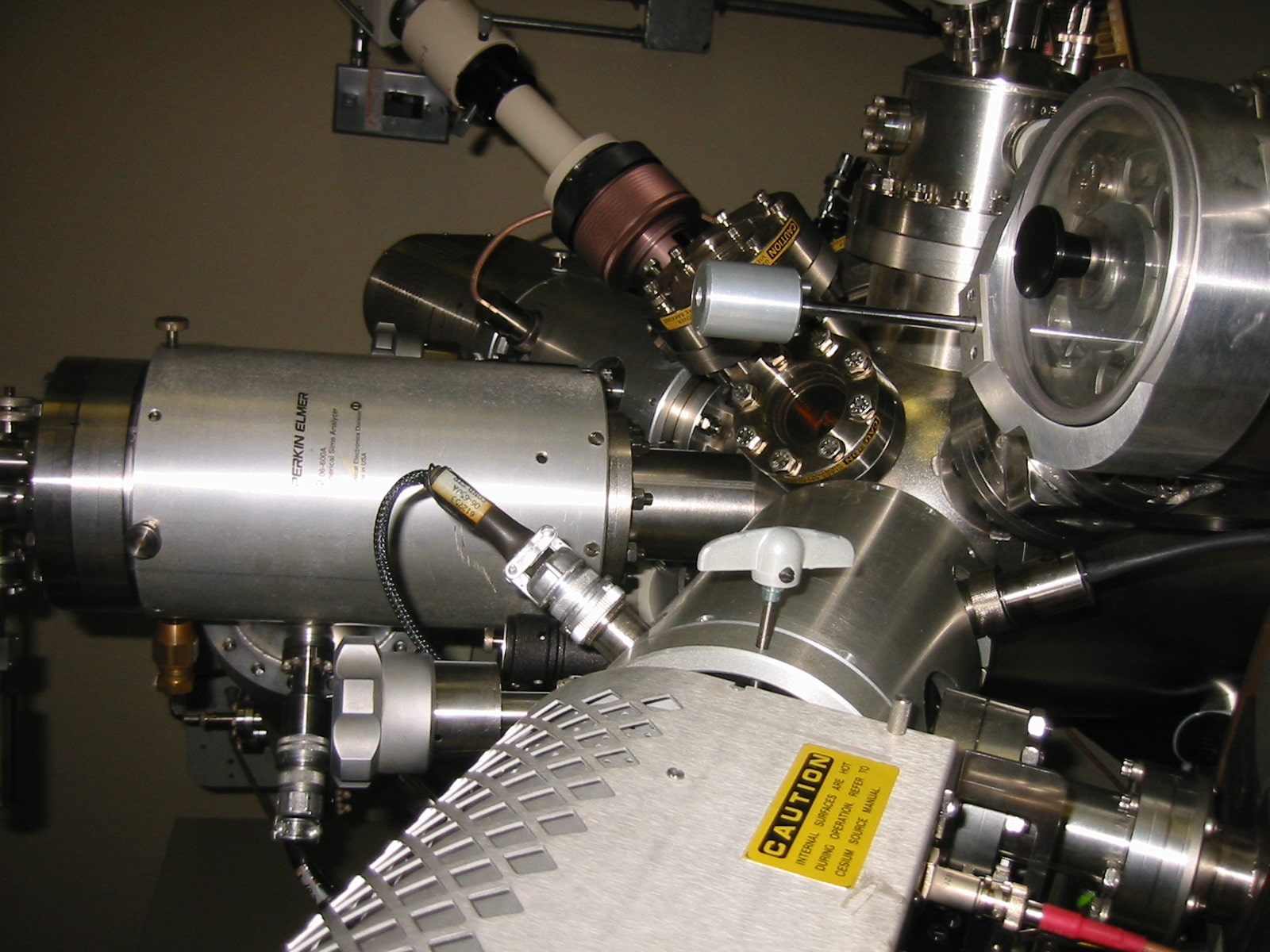
With an extensive range of analysis tools at our disposal (SIMS, XPS, CV profiler, TOF-SIMS, RBS, FIB-TEM), we evaluate your issues and we suggest the most suitable solutions to provide the information you need : doping profiles, impurities presence and concentration, matrix composition, layers thicknesses, interface quality and interdiffusion, doping uniformity, …