Electrochemical CV-Profiling
1. Descritpion
The Electrochemical Capacitance-Voltage (ECV) profiling technique is employed to measure the active carrier concentration profiles in semi-conductor layers.
The technique uses an electrolyte-semiconductor Schottky contact to create a depletion region, a region which is empty of conducting electrons and holes, but contain ionized donors and electrically active defects or traps The depletion region with its ionized charges inside behaves like a capacitor. The measurement of the capacitance provides information of the doping and electrically active defect densities. Depth profiling is achieved by electrolytically etching the semiconductor between the capacitance measurements with no depth limitation.
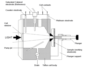
2. The electrochemical cell
The electrochemical cell is schematically shown on figure1.
The sample is pressed against a sealing ring in the electrochemical cell containing an electrolyte. The ring opening defines the contact area. The depletion region is created by applying a potential between the semiconductor and the platinum electrode measured with respect to the reference saturated calomel electrode. The etching conditions are controlled by the current circuit between the semiconductor and the counter electrode.
3. Carrier concentration measurement
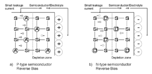
Depending of the charge of the ions in solution adjacent to the interface, carriers may be attracted (accumulation) or repelled (depletion) in the field-affected region. To measure carrier concentration by CV methods, conditions must be such that a region depleted of carriers is formed. For a p-type semiconductor, where the majority carriers are holes, this condition is satisfied by positive ions in solution, as shown in Figure 2. By making the semiconductor more negative than its equilibrium value, positive ions are attracted to the interface and holes are repelled. For a n-type semiconductor, where the majority carriers are electrons, negative ions are required and thus the semiconductor must be made more positive than its equilibrium value (also shown on Figure 2).
From metal/semiconductor junction equations, a linear relantionship between 1/C2 and V, with C the junction capacitance and V the applied voltage:
1C2 = 2(ɸ-V)qNε0εrA2
With:
- ɸ= ‘Built in’ or contact potential
- q= Charge of the electron
- N= Carrier concentration
- ε0= Permittivity of free space
- εr= Relative permittivity of the semiconductor
- A= Effective contact or etch area
The charge carrier density at the edge of the junction depletion layer is therefore given by:
N =1qε0εrA2 x C3dC/dV
Thus, N is determined by the measurement of A, C and dC/dV. Parameters C and dC/dV are obtained by using a slowly modulated high frequency voltage. The area A must be measured precisely.
4. Etching Conditions
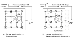
The advantages of using an electrolyte are apparent when the dissolution process is considered. Depth profiling is achieved by dissolving the semiconductor electrolytically, The dissolution process results in an increasing separation of electric charge which depends on the presence of holes. For p-type semiconductors, holes are the majority carriers and dissolution is readily achieved by forward biasing the electrolyte-semiconductor junction. For n-type material, holes are generated by illuminating and reverse biasing the junction. The light with a short enough wavelength promotes electrons from the valence to the conduction band, leaving holes behind that are attracted to the surface by reverse biasing the junction (see figure 3). For this to happen the wavelength λ must obey the condition: λ< hc/ Eg (h: Planck constant, c: light velocity in vacuum, Eg: semiconductor bandgap.
The etched depth Wr depends on the dissolution current I disaccording to the relationship from the Faraday’s law of electrolysis.
Wr = MzFρA ∫ Idis dt
With:
- z= Dissolution valency (number of charge carrier required to dissolve one semiconductor atom)
- F= Faraday constant
- ρ= Semiconductor density
- M= Semiconductor molecular weight
- A= Contact area
The measurement depth of the carrier density is W=Wd+Wr.
5. Measurement procedure
To perform a measure one must:
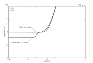
- Obtain an I-V plot, from which it is possible to derive the bias voltage range for capacitance measurement and to indicate the potential to create etching conditions (see figure 4).
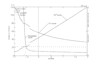
- Perform a C-V curve to obtain the measurement potential (see figure 5).
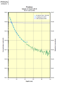
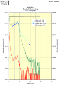
- Using information obtained above, perform the depth profile (see examples of figures 6 and 7).
Examples of doping profiles obtained from ECVP measurements:
6. Performance specifications
- Carrier concentration: 1013cm-3 to 1020cm-3
- Depth range: 0.05µm to 50µm
- Depth resolution: 1nm
- Carrier frequency: 0.3kHz to 25kHz
- Modulation frequency: 0.01kHz to 2.55kHz
7. Limitations
Absolute accuracy of the carrier concentration and etch depth depends on a precise measurement of the contact area. The contact area calibration is therefore critically important. Additional inaccuracies can arise from bubbles in the O-ring or O-ring distortion and wear resulting from unintentional variations in the pressure holding the sample against it. The O-ring must be soft enough to form a seal with variable semiconductor surfaces, but sufficiently rigid to precisely define the Schottky contact area.
The ECV profile measures the « net electrical effect » of the dopant atoms introduced into the epitaxial layer during growth, hence the effective depth resolution is limited to around a Debye length, and is, therefore, inversely proportional to the square root of the doping concentration.
Electrical-contact problems can also introduce measurement variations. To determine capacitance, an ohmic contact is formed either via a back contact to a conducting substrate or directly through a front contact to the epitaxial layers. Contact quality on systems can vary and lead to unreliable results. Other issues can arise from samples with too high a series resistance for the electronics and modelling of the semiconductor-electrolyte interface.